
The Two-Chip Habit: Why Your Wireless Endpoint Doesn’t Need a Host MCU

Published on Jul 22, 2026 in

How hostless architectures cut BOM cost and idle power by running the application where the radio already lives

Open the schematic of a typical battery-powered Wi-Fi endpoint, and you’ll find an architecture that made sense fifteen years ago: a host microcontroller running the application, wired over SPI or UART to a wireless chip acting as a network coprocessor. Two processors. Two firmware images. Two power domains to manage. Two things that can be asleep at the wrong time.

Nobody designed it that way on purpose. The two-chip architecture is a habit inherited from an era when wireless silicon couldn’t be trusted with application code — early Wi-Fi chips had no spare compute, no user-accessible memory, and power budgets that made “always connected” a contradiction in terms. The host MCU existed because it had to.

That constraint is gone. Modern wireless SoCs integrate an application-class processor, memory, security elements, and peripherals alongside the radio. The question worth asking at the start of every new endpoint design is no longer “which host MCU pairs with my radio?” It’s “What is the host MCU still for?”
For a large class of IoT endpoints — sensors, locks, monitors, actuators, trackers — the honest answer is: nothing that justifies its cost.

What the second chip actually costs

The host MCU’s line item on the BOM understates its real price. Count what travels with it.

The silicon and its entourage.

The MCU itself, its decoupling network, its crystal or resonator, often its own flash for firmware storage, and frequently a level shifter or additional regulator because the host and radio don’t share a supply rail. On a cost-sensitive endpoint, this cluster can rival the wireless module itself—and it consumes board area that constrains enclosure design in exactly the product categories (wearables, retrofit sensors, compact locks) where enclosure is destiny.

The interconnect tax.

Every byte the application sends or receives crosses a chip-to-chip link. SPI and UART transfers aren’t free: both processors must be awake for the handoff, the link runs far slower than internal memory buses, and the protocol overhead of framing data across the boundary burns cycles on both sides. In a duty-cycled device, this shows up precisely where it hurts most — extending the awake window on every single transaction, thousands of times over the product’s life.

The coordination problem.

Two processors mean two sleep-state machines that must agree with each other. The design patterns are familiar and familiarly painful: the host wakes the radio and waits; the radio receives data and must wake the host; wake-source GPIOs, handshake lines, and timeout handlers proliferate. Much of the “low-power firmware engineering” on a two-chip endpoint isn’t application work at all — it’s choreography, and every misstep is a field-return-shaped bug that only appears at scale.
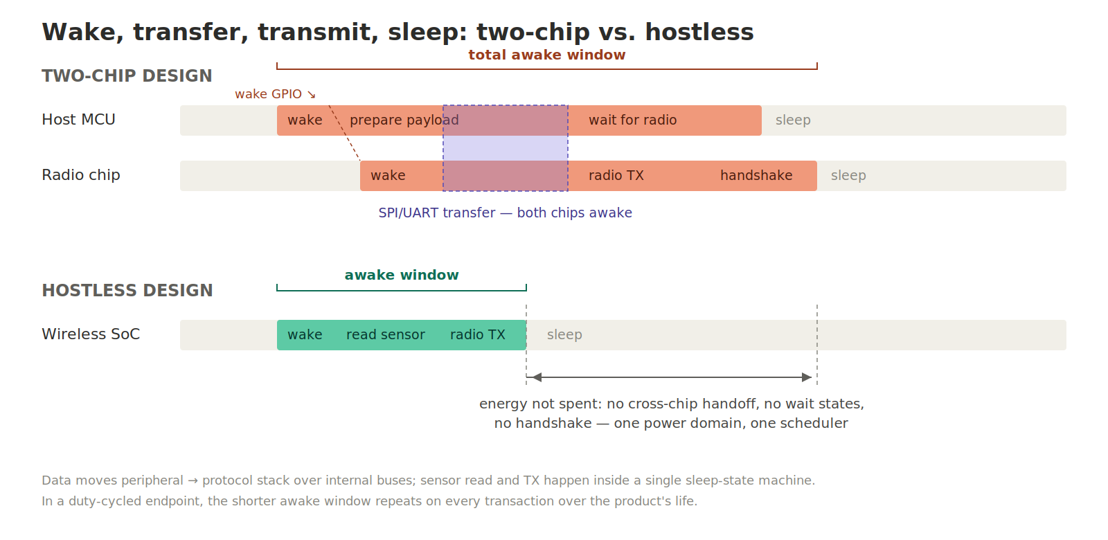
Diagram showing the sleep-state coordination problem between a host MCU and a wireless chip in a two-chip IoT design

The doubled software surface. Two firmware images mean two build systems, two OTA update paths that must stay compatible with each other, and two attack surfaces to secure and patch. For products with a decade of expected field life, the maintenance cost of keeping two codebases in lockstep is a recurring expense that never appears in the BOM.

The hostless alternative

A hostless architecture runs the application directly on the wireless SoC’s embedded processor. On InnoPhase IoT’s breakthrough Talaria platform, this has been a production-proven model since Talaria TWO: the SoC integrated an embedded Arm Cortex-M3 alongside the PolaRFusion™ digital polar radio, with the SDK, FreeRTOS-based environment, and cloud connectivity stacks needed to build the entire endpoint application on-chip. Talaria 6 extends the same model with substantially more processing headroom, more memory, multi-protocol connectivity — Wi-Fi 6, Wi-Fi 7 readiness with MSC15 support, Bluetooth 6, Thread, Zigbee — and Edge AI capability, widening the range of applications that fit comfortably in a single-chip design.

The gains map directly onto the costs above. The MCU and its entourage leave the BOM and the board. The interconnect tax disappears because there is no interconnect — sensor data moves from the peripheral to the protocol stack across internal buses within a single power domain under a single scheduler. Sleep management becomes one state machine rather than a negotiation. And there is one firmware image: one build, one signed OTA path, one attack surface.
There’s a subtler power benefit worth naming. In a two-chip design, the system’s floor current is the sum of two chips’ sleep currents plus whatever leaks through the interconnect and level shifting. In a hostless design, the floor is a single SoC engineered as one power-management domain — which is how ultra-low connected-idle figures translate into system-level battery life instead of being averaged away by a second chip the radio vendor doesn’t control.

A concrete illustration: standalone Matter-over-Wi-Fi devices built on Talaria TWO run the full Matter stack on-chip, connecting directly to the cloud with no external MCU and no Thread border router in the deployment — collapsing not just the board architecture but the network architecture around it. Matter 1.6 will be supported in the Talaria 6 SDK.

The same logic is now surfacing in the industry’s newest credentialing standards. InnoPhase IoT is an active member of the The Connectivity Standards Alliance. The Connectivity Standards Alliance’s specification for mobile access credentials — letting a phone or wearable act as a digital key for a smart lock or access reader — is built around the same on-chip model this article has been making the case for all along: authentication, credential storage, and protocol handling are workloads measured in tens of kilobytes, well within what a connected SoC’s embedded processor was already designed to absorb. For lock and access-reader designs on the Talaria platform, the Bluetooth 6 and Thread connectivity already on-chip is the same connectivity this next generation of credential standards runs on — which means keeping pace with where mobile access credentialing is headed doesn’t require adding a second chip to the design.
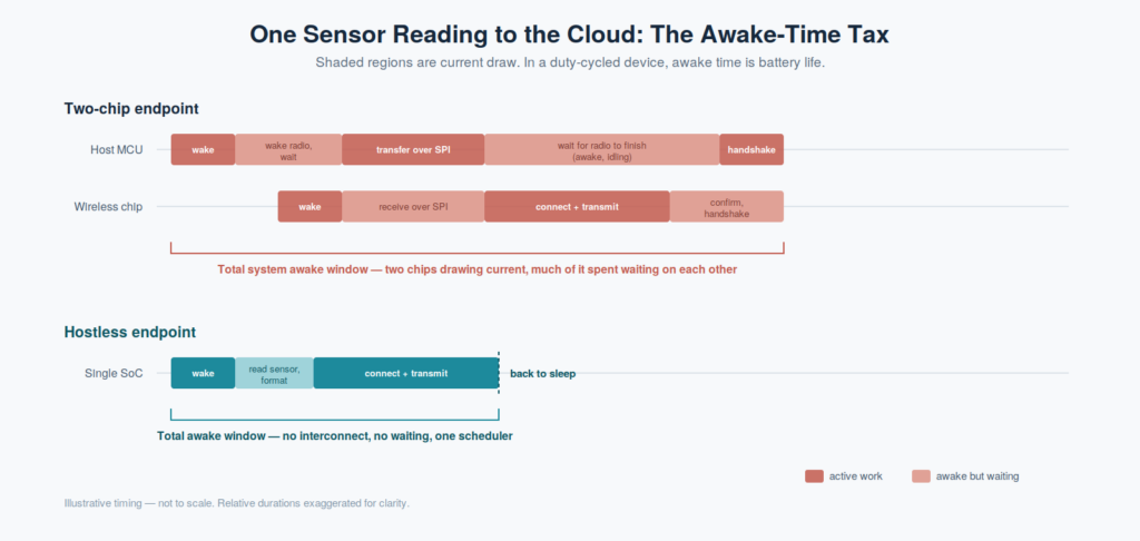
Diagram of a hostless wireless SoC handling authentication, credential storage, and protocol handling on-chip for mobile access credentials

When you still want a host — and why that’s fine

Engineering credibility requires saying the quiet part: hostless is not universal. Applications with heavy compute — video analytics pipelines, large legacy codebases certified on a specific MCU, or workloads that genuinely need a Cortex-M7-class or application processor — will keep a companion chip. And migration reality matters: teams with years of validated code on an existing MCU can’t always rewrite on schedule.

The architecture question isn’t binary, and the platform shouldn’t force it to be. Talaria supports three modes: fully hostless, attached to a host MCU over UART/SPI as a low-power network processor, and a hybrid mode where responsibilities are split — for instance, offloading the entire connectivity and protocol burden (including a full Matter stack) to the wireless SoC so a modest external MCU keeps its memory and cycles for the custom application. That means the same platform serves both the design you’re shipping this year and the leaner one you’re architecting next.
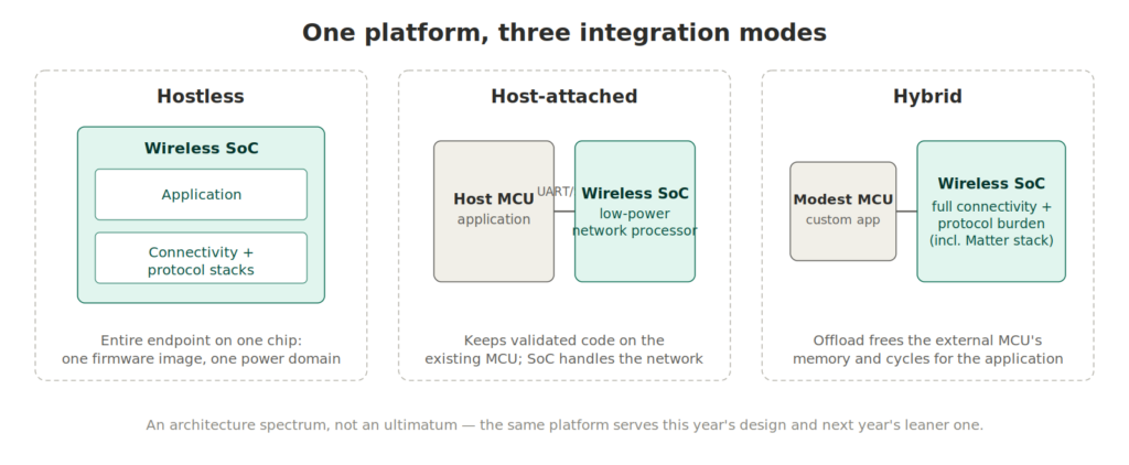
Diagram of three Talaria SoC operating modes: fully hostless, host-attached network processor, and hybrid split-workload

But the default deserves to flip. For the sensor, the lock, the monitor, the tracker — endpoints whose application logic is measured in tens of kilobytes, not megabytes — the second chip is a habit, not a requirement. Every new endpoint design should have to justify the host MCU’s presence, not its absence.

The design review question

At your next architecture review, run the exercise: list what your host MCU does that the wireless SoC’s embedded processor cannot. If the list is “reads sensors, applies logic, formats payloads, manages sleep” — that’s a hostless design wearing a two-chip costume, and it’s costing you board area, BOM lines, idle current, and a second firmware team.

The endpoint of the next decade is single-chip. The only question is whether your product line gets there before your competitor’s cost structure does.

Click here to download the Talaria 6 product brief or contact Sales for a demo or datasheet.

How hostless architectures cut BOM cost and idle power by running the application where the radio already lives

Open the schematic of a typical battery-powered Wi-Fi endpoint, and you’ll find an architecture that made sense fifteen years ago: a host microcontroller running the application, wired over SPI or UART to a wireless chip acting as a network coprocessor. Two processors. Two firmware images. Two power domains to manage. Two things that can be asleep at the wrong time.

Nobody designed it that way on purpose. The two-chip architecture is a habit inherited from an era when wireless silicon couldn’t be trusted with application code — early Wi-Fi chips had no spare compute, no user-accessible memory, and power budgets that made “always connected” a contradiction in terms. The host MCU existed because it had to.

That constraint is gone. Modern wireless SoCs integrate an application-class processor, memory, security elements, and peripherals alongside the radio. The question worth asking at the start of every new endpoint design is no longer “which host MCU pairs with my radio?” It’s “What is the host MCU still for?”
For a large class of IoT endpoints — sensors, locks, monitors, actuators, trackers — the honest answer is: nothing that justifies its cost.

What the second chip actually costs

The host MCU’s line item on the BOM understates its real price. Count what travels with it.

The silicon and its entourage.

The MCU itself, its decoupling network, its crystal or resonator, often its own flash for firmware storage, and frequently a level shifter or additional regulator because the host and radio don’t share a supply rail. On a cost-sensitive endpoint, this cluster can rival the wireless module itself—and it consumes board area that constrains enclosure design in exactly the product categories (wearables, retrofit sensors, compact locks) where enclosure is destiny.

The interconnect tax.

Every byte the application sends or receives crosses a chip-to-chip link. SPI and UART transfers aren’t free: both processors must be awake for the handoff, the link runs far slower than internal memory buses, and the protocol overhead of framing data across the boundary burns cycles on both sides. In a duty-cycled device, this shows up precisely where it hurts most — extending the awake window on every single transaction, thousands of times over the product’s life.

The coordination problem.

Two processors mean two sleep-state machines that must agree with each other. The design patterns are familiar and familiarly painful: the host wakes the radio and waits; the radio receives data and must wake the host; wake-source GPIOs, handshake lines, and timeout handlers proliferate. Much of the “low-power firmware engineering” on a two-chip endpoint isn’t application work at all — it’s choreography, and every misstep is a field-return-shaped bug that only appears at scale.

Diagram showing the sleep-state coordination problem between a host MCU and a wireless chip in a two-chip IoT design

The doubled software surface. Two firmware images mean two build systems, two OTA update paths that must stay compatible with each other, and two attack surfaces to secure and patch. For products with a decade of expected field life, the maintenance cost of keeping two codebases in lockstep is a recurring expense that never appears in the BOM.

The hostless alternative

A hostless architecture runs the application directly on the wireless SoC’s embedded processor. On InnoPhase IoT’s breakthrough Talaria platform, this has been a production-proven model since Talaria TWO: the SoC integrated an embedded Arm Cortex-M3 alongside the PolaRFusion™ digital polar radio, with the SDK, FreeRTOS-based environment, and cloud connectivity stacks needed to build the entire endpoint application on-chip. Talaria 6 extends the same model with substantially more processing headroom, more memory, multi-protocol connectivity — Wi-Fi 6, Wi-Fi 7 readiness with MSC15 support, Bluetooth 6, Thread, Zigbee — and Edge AI capability, widening the range of applications that fit comfortably in a single-chip design.

The gains map directly onto the costs above. The MCU and its entourage leave the BOM and the board. The interconnect tax disappears because there is no interconnect — sensor data moves from the peripheral to the protocol stack across internal buses within a single power domain under a single scheduler. Sleep management becomes one state machine rather than a negotiation. And there is one firmware image: one build, one signed OTA path, one attack surface.
There’s a subtler power benefit worth naming. In a two-chip design, the system’s floor current is the sum of two chips’ sleep currents plus whatever leaks through the interconnect and level shifting. In a hostless design, the floor is a single SoC engineered as one power-management domain — which is how ultra-low connected-idle figures translate into system-level battery life instead of being averaged away by a second chip the radio vendor doesn’t control.

A concrete illustration: standalone Matter-over-Wi-Fi devices built on Talaria TWO run the full Matter stack on-chip, connecting directly to the cloud with no external MCU and no Thread border router in the deployment — collapsing not just the board architecture but the network architecture around it. Matter 1.6 will be supported in the Talaria 6 SDK.

The same logic is now surfacing in the industry’s newest credentialing standards. InnoPhase IoT is an active member of the The Connectivity Standards Alliance. The Connectivity Standards Alliance’s specification for mobile access credentials — letting a phone or wearable act as a digital key for a smart lock or access reader — is built around the same on-chip model this article has been making the case for all along: authentication, credential storage, and protocol handling are workloads measured in tens of kilobytes, well within what a connected SoC’s embedded processor was already designed to absorb. For lock and access-reader designs on the Talaria platform, the Bluetooth 6 and Thread connectivity already on-chip is the same connectivity this next generation of credential standards runs on — which means keeping pace with where mobile access credentialing is headed doesn’t require adding a second chip to the design.

Diagram of a hostless wireless SoC handling authentication, credential storage, and protocol handling on-chip for mobile access credentials

When you still want a host — and why that’s fine

Engineering credibility requires saying the quiet part: hostless is not universal. Applications with heavy compute — video analytics pipelines, large legacy codebases certified on a specific MCU, or workloads that genuinely need a Cortex-M7-class or application processor — will keep a companion chip. And migration reality matters: teams with years of validated code on an existing MCU can’t always rewrite on schedule.

The architecture question isn’t binary, and the platform shouldn’t force it to be. Talaria supports three modes: fully hostless, attached to a host MCU over UART/SPI as a low-power network processor, and a hybrid mode where responsibilities are split — for instance, offloading the entire connectivity and protocol burden (including a full Matter stack) to the wireless SoC so a modest external MCU keeps its memory and cycles for the custom application. That means the same platform serves both the design you’re shipping this year and the leaner one you’re architecting next.

Diagram of three Talaria SoC operating modes: fully hostless, host-attached network processor, and hybrid split-workload

But the default deserves to flip. For the sensor, the lock, the monitor, the tracker — endpoints whose application logic is measured in tens of kilobytes, not megabytes — the second chip is a habit, not a requirement. Every new endpoint design should have to justify the host MCU’s presence, not its absence.

The design review question

At your next architecture review, run the exercise: list what your host MCU does that the wireless SoC’s embedded processor cannot. If the list is “reads sensors, applies logic, formats payloads, manages sleep” — that’s a hostless design wearing a two-chip costume, and it’s costing you board area, BOM lines, idle current, and a second firmware team.

The endpoint of the next decade is single-chip. The only question is whether your product line gets there before your competitor’s cost structure does.

Click here to download the Talaria 6 product brief or contact Sales for a demo or datasheet.

Scroll to Top